

Big breakthrough! Chinese research team successfully prepared the world's first!
发布时间 : 2024-01-05
January 4 news, recently, the research team of Tianjin International Research Center for Nanoparticles and NanoSystems under Tianjin University, together with researchers from Georgia Institute of Technology in the United States, overcame the biggest obstacle to graphene research for decades, successfully created the world's first functional semiconductor made of graphene, in the silicon-based semiconductor miniaturization has been close to the limit of the present, It opens a new door for the development of the semiconductor industry.
Breaking through decades of technical barriers, the world's first graphene semiconductor was born!
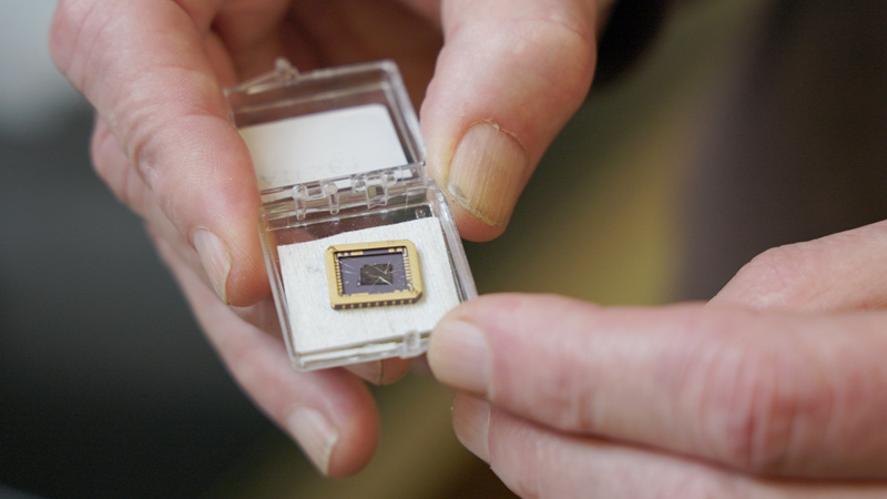
△ Graphene devices grown on silicon carbide substrate prepared by the research team
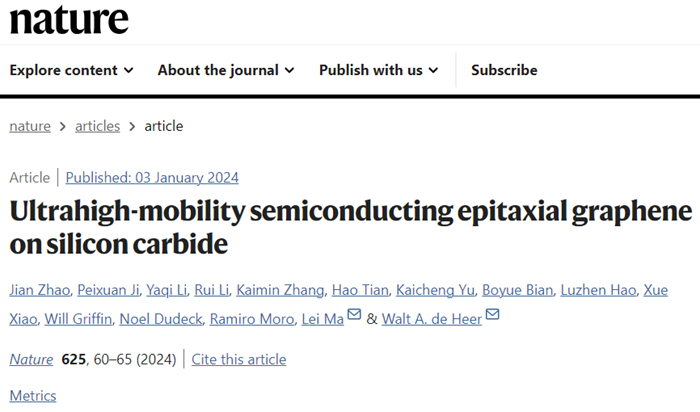
The current paper associated with the study, Ultrahigh mobility semiconducting epitaxial graphene on silicon carbide (" Ultra-High Mobility semiconductor epitaxial Graphene on Silicon Carbide ") has been successfully published in the journal Nature, the co-first authors of the paper are Zhao Jian, Ji Peixuan, Li Yaqi, Li Rui four people, the rest of the signatories are mainly from the Tianjin University research team in China. There are also researchers led by Walter de Heer, a professor at Georgia Institute of Technology in the United States.
Breaking through decades of technical barriers, the world's first graphene semiconductor was born!
It is understood that the graphene semiconductor research is led by the Tianjin University team, not by Walter DeHerr, a physics professor at Georgia Institute of Technology, as reported by some foreign media. The research team was supervised by Ma Lei, professor of Tianjin University and executive director of Tianjin International Research Center for Nanoparticles and Nanosystems. The main research and research work were completed by the Chinese team, and Walter DeHerr proposed the research direction.
Data show that Graphene is an allotrope of carbon, carbon atoms to sp² hybrid bond to form a single hexagonal honeycomb lattice graphene, only one atom of ultra-thin thickness, is a two-dimensional material, not only strong and durable, but also can handle very large currents, and will not heat up and decompose. All of these characteristics suggest that graphene is an ideal material for the preparation of future faster, smaller and more energy efficient electronic components, and another major advantage is that the raw material for preparing graphene is theoretically available in unlimited supply.
However, graphene, which is neither a semiconductor nor a metal but a semi-metal, does not have the right "band gap" (the difference in energy between the lowest point of the conduction band and the highest point of the valence band) to turn on and off at the right ratio when an electric field is applied - the biggest obstacle that has plagued research into graphene-related semiconductors. So the main problem in graphene electronics research is how to open the "band gap" and achieve the function of on and off, so that it can have semiconductor properties like silicon, so that it can work.
In the past two decades, many researchers have tried to open the "band gap" of graphene through various methods, but have failed to prepare feasible graphene-based functional semiconductors, which will largely lose the intrinsic properties of the material.
In this regard, the research team of Tianjin University obtained semiconductor properties by epitaxial graphene on a silicon carbide wafer, that is, growing a single layer of graphene on a silicon carbide wafer and making it chemically bonded with silicon carbide.
The summary of the paper states: "It is well known that when silicon evaporates from the surface of a silicon carbide crystal, the carbon-rich surface crystallizes to produce multiple layers of graphene. The first graphene layer formed on the silicon terminal of silicon carbide is an insulating apparent graphene partially covalently bound to the surface of silicon carbide. Spectral measurements of this buffer layer demonstrate the semiconductor signal, but because it is disordered, the electron mobility of this layer is limited. Here, the research team demonstrated a quasi-equilibrium annealing method that produces semiconductor graphene (i.e., ordered buffer layers) on a flat platform of macroscopic atoms. Semiconductor graphene lattices aligned with silicon carbide substrates are chemically, mechanically and thermally stable and can be patterned and seamlessly connected to graphene semiconductors using conventional semiconductor manufacturing techniques. These fundamental properties make semiconducting graphene suitable for nanoelectronics."
Professor Marley also said: "The long-standing problem in graphene electronics is how to open the band gap while maintaining the high mobility characteristics of graphene materials. Our research has solved this problem, which is a key step towards the application of graphene electronics in electronic products."
But to make a functional graphene transistor, a lot of manipulation must be done with the material, which can compromise its performance. Because graphene is only one atom thick, all atoms are important, and even tiny irregularities in the pattern can destroy its properties. To prove that their platform could function as a viable semiconductor, the research team needed to measure its electronic properties without damaging it.
According to the team's measurements, the graphene semiconductor they prepared on silicon carbide has a band gap of 0.6 eV and room temperature electron mobility of more than 5,000 cm 2 V-1 s-1, which is 10 times that of silicon and 20 times that of other two-dimensional semiconductors. In other words, electrons can move with very low drag, which in electronics means faster computing power. Moreover, thanks to the two-dimensional characteristics of graphene itself, it has better heat dissipation performance and higher efficiency. The graphene semiconductor is also currently the only two-dimensional semiconductor with all the necessary properties for nanoelectronics, and its electrical properties are far superior to any other two-dimensional semiconductor currently under development.
"It's like a Wright Brothers moment for me." Professor Walter DeHerr said: "It's like building a plane that can fly 300 feet in the air. But skeptics ask why the world needs planes when it already has high-speed trains and ships. But they persevered, and this is the beginning of a technology that can take people across the world."
Epitaxial graphene could cause a paradigm shift in electronics, allowing researchers to exploit its unique properties to study entirely new semiconductor technologies. At the same time, the production method of the graphene semiconductor can be compatible with the traditional silicon-based semiconductor manufacturing method, which is also a necessary condition for the graphene semiconductor to replace the silicon-based semiconductor.
The researchers wrote in the paper that the technology has "significant potential for commercial viability in the future."
In an interview with the First financial industry, Ma Lei also said that if this material is put into industrial applications, in terms of cost, it is basically comparable to the semiconductor manufacturing materials on the market now, and in terms of performance, it will be more superior.
Still, there are a lot of issues that need to be resolved before graphene semiconductors can be extended to computing chips.
"I estimate it will be another 10 to 15 years before we can really see graphene semiconductors fully landing." Marley said the research team is working to try to make graphene semiconductor materials grow on a larger size of silicon carbide substrate.